The move comes as hyperscalers and AI data centres hoover up memory at an unprecedented pace, so there is a market for this.
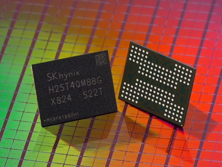
The company says the chip doubles the capacity of its existing solutions and boosts performance by reworking the internal architecture. By expanding the number of planes inside each chip from four to six, SK hynix says it has solved some of the sluggishness typically associated with bloated QLC. That trick enables more parallel operations, faster reads, and much less of the crawl QLC is known for.
According to SK hynix's numbers, write performance is up 56 per cent, reads are up 18 per cent, and overall transfer speeds have doubled compared with its last-gen parts. Power efficiency during writes has improved by 23 per cent, which the company reckons makes it more attractive for data-centre buyers keeping an eye on their electricity bills.
SK hynix head of NAND development Jeong Woopyo said the launch strengthens its high-capacity portfolio.
“We will make a major leap forward as a full-stack AI memory provider, in line with the explosive growth in AI demand and high-performance requirements in the data center market,” he said.
The first products to get the new NAND will be consumer PC SSDs, with enterprise SSDs for data centres and UFS storage for smartphones following later. The firm plans to combine its 321-layer chips with its in-house 32DP packaging tech, which stacks up to 32 dies in one package, to build monster-sized eSSDs for AI servers with twice the integration density.