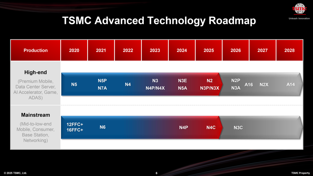
Unveiled at TSMC’s North American Technology Symposium 2025, A14 is described by the company’s senior vice president and deputy COO, Kevin Zhang, as “our full-node next generation advanced silicon technology.” That’s corporate speak for a significant leap beyond N2, not just a dressed-up refresh.
“Speed enhancement compared to N2 is up to 15 per cent, power reduction is at 30 per cent, logic density is 1.23x the overall chip density, or at least 1.2x for mixed designs,” Zhang said.
A14 uses TSMC’s 2nd Generation GAA (gate-all-around) nanosheet transistors—a key update from the first-gen GAA seen in the N2 series. Additionally, TSMC is introducing NanoFlex Pro, a new design technology co-optimisation tool that expands on the FinFlex concept.
While the foundry was thin on the details, the implication is greater design granularity and control for chip engineers, likely involving better libraries, refined EDA software, or potentially transistor-level configurability.
The node promises up to 15 per cent performance improvement at the same power and design complexity, or a 25 to 30 per cent power reduction at the same performance level, when compared to N2.
Density also sees a lift: up to 23 per cent for pure logic and 20 per cent for mixed chip designs (a standard cocktail of 50 per cent logic, 30 per cent SRAM, 20 per cent analog).
This first iteration of A14 will stick with front-side power delivery. That means no Super Power Rail (SPR), also known as backside power delivery network (BSPDN), which is featured in TSMC’s forthcoming A16 node. This means that there will be a reduced cost and complexity for customers whose applications don’t benefit dramatically from backside routing—think mobile, consumer, edge, and IoT silicon rather than hyperscaler-grade compute.
TSMC acknowledges the need for backside power in high-performance computing, though. A version of A14 with SPR is due in 2029, and while they haven’t confirmed it, it’ll likely go by A14P, following the same naming logic as N4P, N3P, and others in the TSMC zoo. Once SPR enters the frame, expect that flavour of A14 to go after data centre workloads and AI accelerators with a vengeance.
The foundry has hinted that additional variants, like A14X for maximum performance and A14C for cost-sensitive deployments, may follow after 2029, allowing customers to scale up or down the power ladder as needed.
TSMC’s roadmap puts A14 mass production in 2028. While the company didn’t clarify whether volume starts in the first or second half of the year, all signs point to an H1 2028 launch. With N2P and A16 headed for production in late 2026, a mid-2028 rollout would keep TSMC’s cadence tight and ensure A14-based chips can hit the shelves by late 2028, just in time for next-gen smartphones, laptops, and edge devices to debut.
TSMC is charging ahead with a node that isn’t just denser—it’s smarter. But until the SPR version arrives, the high-end compute crowd may wait for the full-fat version.
Advertised PPA Improvements of TSMC's New Process Technologies
|
Row 0 - Cell 0 |
A16 vs N2P |
N2X vs N2P |
A14 vs N2 |
A14 SPR vs N2 |
|
Power |
-15% ~ -20% |
lower |
-25% ~ -30% |
lower |
|
Performance |
8% - 10% |
10% |
10% - 15% |
higher |
|
Density* |
1.07x - 1.10x |
? |
1.2x |
denser |
|
Transistor |
GAA |
GAA |
2nd Gen GAA |
2nd Gen GAA |
|
Power Delivery |
SPR |
Front-side w/ SHPMIM (?) |
Front-side w/ SHPMIM (?) |
SPR |
|
HVM |
H2 2026 |
2027 |
2028 |
2029 |
*TSMC's chip density publication reflects a 'mixed' chip density consisting of 50% logic, 30% SRAM, and 20% analogue.
**At the same area.
***At the same speed.