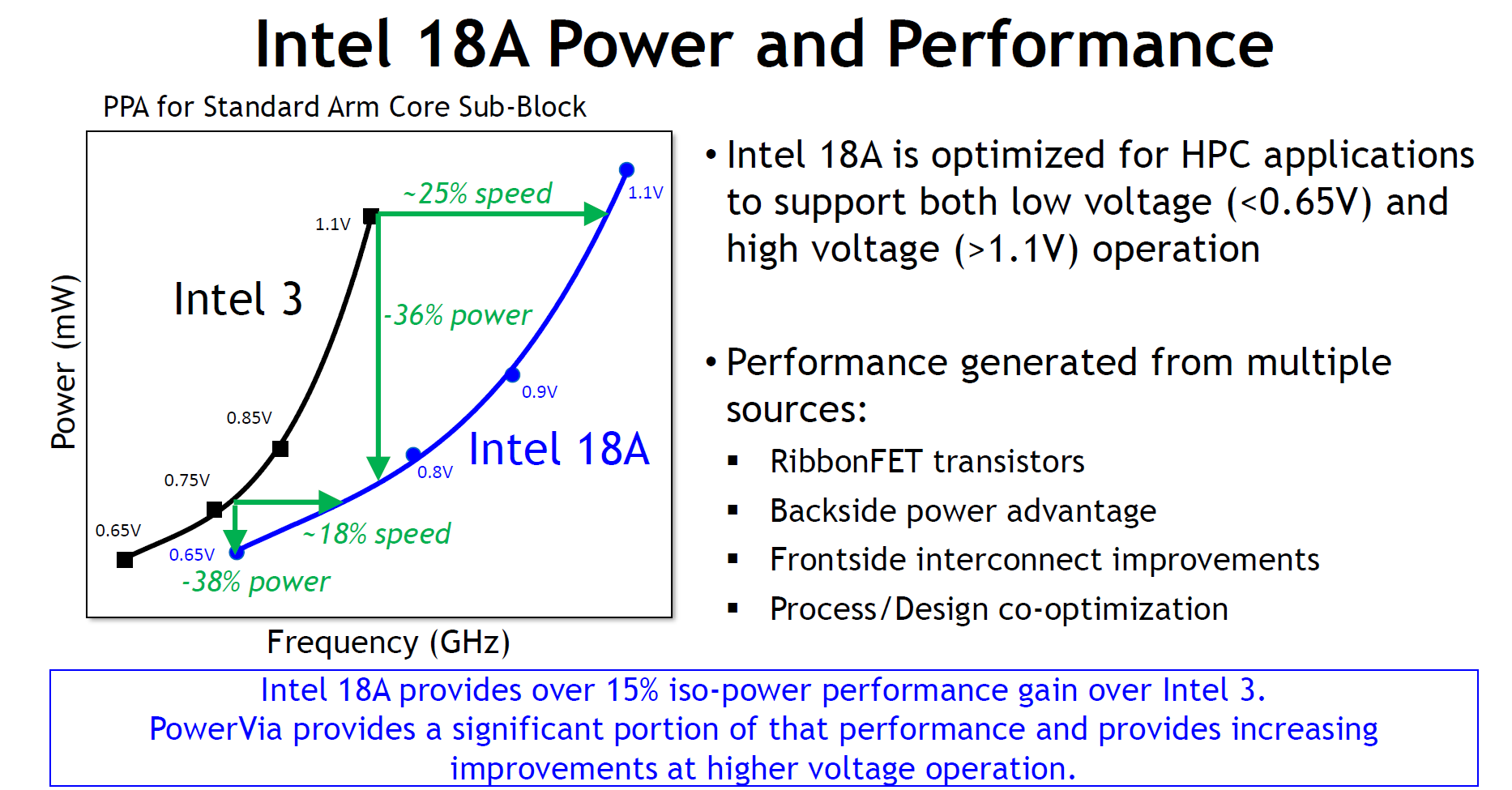
According to Intel, the 18A node, which will underpin upcoming “Panther Lake” client CPUs and “Clearwater Forest” E-core-only Xeon parts, will be a major leap over Intel 3. Intel says it delivers up to 25 per cent higher frequencies at the same 1.1V voltage and 36 per cent lower power consumption at equivalent clocks, plus more than 30 per cent density scaling.
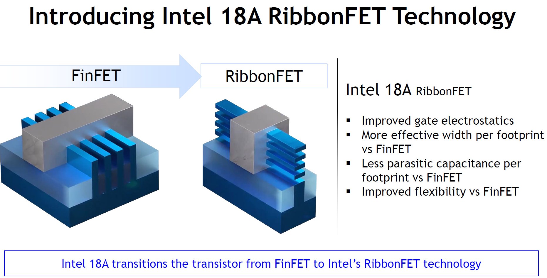
This node introduces RibbonFET gate-all-around transistors and PowerVia backside power delivery, which the company claims brings substantial gains in logic density, interconnect performance and voltage stability. Intel insists this combination marks a full node improvement in both performance and efficiency.
With multiple ribbon widths tailored for logic and SRAM cells, the 18A platform is designed for flexibility. Intel also claims improved cell utilisation and reduced voltage droop, with its new power delivery layout helping cut worst-case IR droop tenfold. The backside power method also untangles power and signal routing layers, boosting design headroom.
The specs include HP and HD library heights of 180nm and 160nm respectively, a contacted poly pitch of 50nm, and metal pitch at M0 down to 32nm. Standard cell area for HCC/HDC SRAM has been squeezed to 0.0230 and 0.0210 μm².
Looking ahead, Intel said it plans to roll out further refinements with 18A-P and 18A-PT nodes between 2026 and 2028. These will be targeted at customers planning to deploy advanced chips using these process variants.
Despite these technical advances, Intel still has to prove it can deliver 18A chips on time and in volume, especially with its foundry business in cost-cutting chaos and CHIPS Act subsidies still hanging in the air.