
According to Taiwanese outlet Ctee, the node now matches the company’s mature 5nm yields and is on course for mass production by the final quarter of 2025. TSMC’s next big node leap comes with a switch to GAAFET (gate-all-around field-effect transistor) architecture. The move away from FinFET means each transistor now gets a nanosheet structure fully wrapped by gate material, which improves density, reduces leakage and trims power usage. It’s the company’s first time using GAAFET in production chips.
AMD will be the first to cash in, having already completed tape-out for its next-generation EPYC chip, codenamed Venice. It’s expected to be the launch showcase for the 2nm node, ahead of Apple’s iPhone 18 and Intel’s Nova Lake CPUs which are slated to use TSMC’s tech.
The client list reads like a who’s who of chip design royalty. Apple, AMD, Intel, NVIDIA, Qualcomm, MediaTek and Broadcom have all booked capacity. NVIDIA’s Rubin GPUs will start life at 3nm but may get a 2nm refresh further down the line.
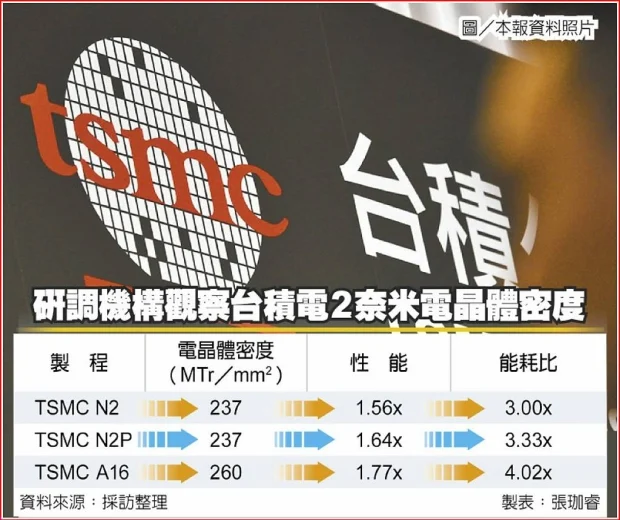
TSMC chairman C.C. Wei called the demand for 2nm “unprecedented,” far outstripping the scramble for 3nm. The shift to GAAFET is seen as the biggest jump in transistor design since the FinFET era began.
Following the 2nm node, TSMC plans to roll out its A14 node in 2028. It will include second-generation nanosheet transistors, offer up to 15 per cent more performance per watt and cut power consumption by as much as 30 per cent at the same frequency.